

Gencoa R&D Commercial Services
Practical services cover PVD & PECVD layer development, plasma etching / cleaning studies, and chemical sensing from vacuum and atmosphere.
Simulation and design services include redesigning magnetic packs for different layer properties on wafers, and modelling magnetic fields and layer uniformity for different process and system types.
A highly experienced R&D team boast expertise in 2D and 3D modelling, electronics, software design, process feedback control, spectroscopic chemical sensing, plasma modelling and measurement, PVD & CVD layer creation on 2D and 3D parts, etch and cleaning of surfaces.
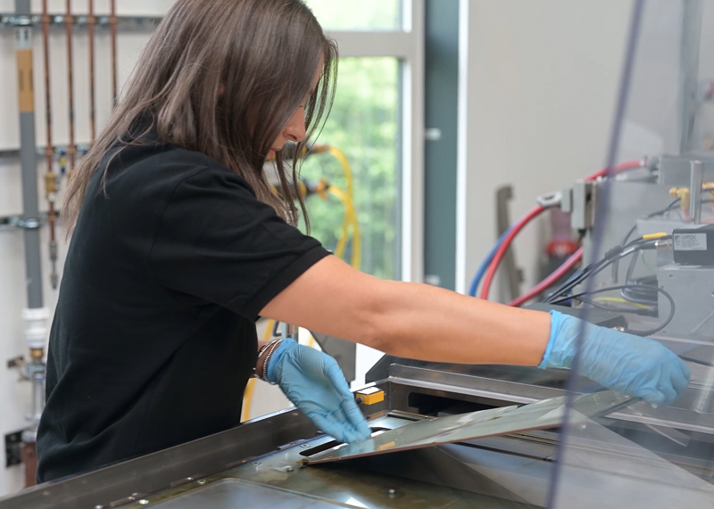
There are eight vacuum development machines at Gencoa that encompass small scale coating on slides or 50mm diameters wafers, 0.5m in-line glass, to 1.2m long 3D parts, and 2.5m long plasma test and treatment.
The scope of work can range from new concepts to pilot production, and be carried out in a single day or involve a project lasting for several months. In addition to in-house development, staff can also work at the customer sites for final process tuning and product testing / staff training.
To discuss requirements relating to new products or improvements to existing products, please use the enquiry button.
Some examples of process work undertaken recently are listed below, and highlight some of our areas of specialisation:
- High pressure plasma cleaning of debris on glass
- Transparent abrasion resistant large window coating development
- Low voltage (180V) sputtered ITO from rotatable targets
- Scratch resistant transparent carbon on phone displays (major area of activity in collaboration with Nano4Energy)
- Remote sensing of deuterium (OPTIX based)
- Cannabinoid sensing from atmosphere (OPTIX based)
- Sensing of automotive battery leaks (OPTIX based)
- Simulation of layer uniformity on large astronomical telescopes
- Highly biocidal coatings on visual displays, food packaging and healthcare products (major area of activity)
- Novel layer stacks for off-grid power generation
- Rapid plasma etching of 3D parts and surfaces (in collaboration with N4E)
- Stress control of layers used in microelectronics
- Magnetic design and testing for 200 and 300mm wafer coating improvements (major area)
Success is a result of skills, facilities and speed. In vacuum deposition and plasma processes we excel in all areas
